24.04.2020by Christos Zachariadis
Fabricating a superconducting quantum processor in a cleanroom

by Christos Zachariadis
Nowadays, quantum computers promise to be a revolutionary technology. As a result, quantum computing has become one of the hottest areas of research in the last decade. A lot of effort has been made on all layers of this new computer stack; from the creation of quantum algorithms to the development of hardware for devices. Lately, the bottleneck of the latter one starts to become more troublesome. Fabricating a growing number of qubits is increasingly difficult and samples are hard to reproduce on a large scale. In this blogpost, we’ll discuss the origins and the difficulties of fabricating a superconducting quantum processor.
In order to guide you through the fab step by step, we have to start from its origin in related disciplines. A quantum computer chip is an integrated circuit. The integrated circuit industry and all related industries, such as microsystems/MEMS, solar cells, flat-panel displays and optoelectronics, rely on microfabrication technologies. Typical dimensions of structures fabricated with microfabrication technologies are around 1μm in the plane of the wafer (ranging from 0.1μm to 100 μm), while the vertical dimensions range from atomic-layer thickness (0.1 nm) to hundreds of micrometres, with typical values are between 10 nm and 1μm.

Fig 1.1 Comparison of scales
Nanotechnology is an outgrowth extension of microfabrication. Some of the tools are still the same, like the electron-beam lithography machines, which were used to design nanometre-sized structures way before the term nanotechnology was coined. Moreover, some of the methods are based on scanning probe devices, such as the atomic force microscope (AFM), which is an important instrument for microstructure characterization. Thin films down to atomic-layer thicknesses have been grown and deposited in the microfabrication communities for decades. Novel ways of depositing films, like self-assembled monolayers (SAMs), have been introduced by nanotechnologists, and some of those techniques are now being investigated by the established microfabrication community as tools for continued downscaling of microstructures.

Figure 1.2: All the involved micro technology fields.
Micrometre-scale structures can be easily destroyed by particles from the surroundings. Moreover, lithography is fragile and can be readily ruined by mechanical vibrations in the environment, or by temperature and humidity fluctuations. Therefore, microfabrication takes place under carefully regulated conditions to achieve a desired level of particle purity. Also, environmental temperature, humidity and vibrations are carefully controlled. Initially, cleanrooms were a solution to particle contaminations. Later on, temperature and humidity fluctuations were also recognized as being harmful for lithography and the control of them for improved reproducibility in lithography was added to cleanroom facilities. Other cleanroom features have been added over the years, and a modern cleanroom is a system of facilities that ensures contamination-free processing under very stable environmental conditions.
There are several ways to ensure such conditions. In Figure 1.3, two cleanroom designs are shown: either high-efficiency filters can be placed locally (right), or they can have 100% coverage (left), offering improved cleanliness and laminar (unidirectional) airflow.
Particle size distributions in a cleanroom environment, in process gases, in DI-water and in wet chemicals all have the same basic characteristics: four to eight times more particles are detected if the detection threshold size is halved. Therefore, if the minimum linewidth is halved, the number of particles that are potential killers increases by four to eight times.
Wafers are cleaned actively during processing: hundreds of litres of ultrapure water (de-ionized water, DIW) are used for each wafer during its fabrication. This is the dynamic part of particle cleanliness, while the passive part comes from materials used for cleanroom walls, floors and ceilings which also includes the sealants and the paints, plus process equipment, wafer storage boxes and all associated tools etc.

Figure 1.3: (Left) high-efficiency filter and (right) high-efficiency air filter cleanroom design.
We learned from the computer industry that the fabrication of microchips is a fragile, yet sophisticated process. And even though extreme care is taken to ensure cleanliness during micro processing, some devices will always be defective. In fact, as the number of process steps increases, the yield goes down exponentially as Y=Y_o^n, where Yo is the yield of a single process step and n is the number of process steps. Imagine that you have 99% yield per individual process step. With, for example, 100 process steps (as is the case for a 64 kbit memory chip), the overall sample yield will be 37%. However, the same 99% yield for a 500-step process (representative of a 16 Mbit memory chip) will result in a total yield smaller than 1%. Since over 500 process steps will be required for chips with larger memories, clearly, 99% yield per individual step is not enough for modern memory fabrication.
Chip design also affects yield through area: Y = exp(−DA) where A is the area of the chip and D is the defect density. As you can see, making small chips is much easier than making big chips. The defect density yield has two major components: stochastic and systematic. Examples of stochastic (random) defects are unpredictable occurrences of pinholes in protective films, particle adhesion on the wafer, corrosion of metal lines, and so on. Systematic defects come from equipment and operator failures, impurities in starting materials, design errors (two features are placed so close to each other that they will inadvertently touch), or impurities in chemicals that do not allow low enough leakage currents.
Having examined some of the basic principles of micro-/nano-fabrication, we can take a closer look at specific problem pertaining to the fabrication of a quantum computer. The quest for fabricating a quantum computer has been inspired by the recognition of the formidable power such a device could offer. Making such devices requires atomic scale manipulation and careful processing for every step until the final assembly of the device. In other words, lots of work hours spent in cleanroom facilities to have the best and the cleanest organic-free quantum processor device.
A normal fabrication process usually starts with the substrate material which, in most of the cases, is silicon (other substrates, like diamond, sapphire, can also be used). Whereas the substrate can have different properties that depends on what quantum processor type the device is meant to be, those properties usually involve the orientation, the material resistivity, the substrate thickness etc. Patterning processes that define structures, as in our case for a quantum processor which involves structures like CPW (coplanar wave guides), flux lines, resonators, transistors, Josephson junctions etc., is usually done in two steps: photolithographic patterning of a resist film (negative or positive), which then acts as a mask for etching or modification of the underlying material Figure 1.4). A photomask defines areas where the photosensitive film (the photoresist) will be exposed. This photoresist will then serve as a mask for subsequent steps. Before this step, according to the final use of the device, cleaning steps can be introduced, followed by the deposition of other metal substrates (Figure 1.5), which is usually used either for protecting or for enhancing the properties of the final device.

Figure 1.4: (a) SiO2 deposition; (b) photoresist application, (c) UV exposure using a photomask, (d) development of resist image, (e) etching of oxide and (f) photoresist removal.
After the pattern is revealed, the resist is stripped away either using an oxygen plasma process or with an organic solution. In this step, preserving your substrate pattern has been one of the main focus in this field as intrinsic loses can seriously decrease the coherence time T1. Here, T1 is a measure of typically how long quantum states that represent qubits remain coherent. Longer times are preferable as this will give more time to complete a quantum operation or more operations to take place in a given algorithm. Preserving a clean substrate-metal interface can be tough as harsh treatment is usually used to achieve a residue-free surface.

Figure 1.5: Example of deposited films on a substrate.
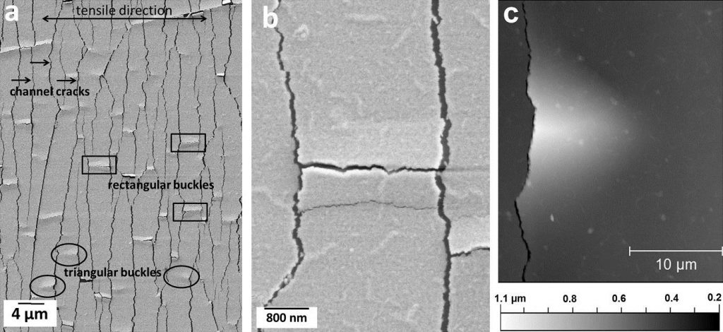
One of these processes are common cleaning techniques that are widely used in the semiconductor industry like RCA-1, RCA-2, piranha wet etching or either different ratios of other chemicals that usually depends on the type of the metal that is used for the base pattern like aluminum (Al), titanium nitride (TiN) and niobium (Nb). This has been always a struggle for a research/process engineer in this field, as nano-structured patterns are extremely sensitive in such conditions, which can easily lead to catastrophic failures like over-etching, re-deposition in unwanted areas of the device or delaminating the metal film from the substrate (Figure 1.6).

Fig 1.6: Examples of delamination of a thin film after over etching.
In conclusion, the current challenges to fabrication of quantum computing hardware is essentially transitioning from a small-scale, academically driven status quo to an industrially viable breakthrough. The current research pursuit is to achieve a scalability formula analogous to the semiconductor integrated circuits which grew from a handful of transistors to packing a few billion in a matter of six decades. New techniques or combination of methods that are already used from other fields like semiconductor industry are being tested every day worldwide, to improve the quality of the qubit interface as well as the scalability of quantum processors. Our task is cut out to pushing the limits of nanofabrication and inventing new ways to avoid problems such as particle accumulation and achieve control of each fabrication process with high accuracy.

Hello everyone and welcome once again to another edition of the QuTech blog! My name is Christos, but you can also call me Chris if its more efficient for you. I am a nanofabrication engineer at Leo DiCarlo’s group.
When I am not in the cleanroom, well I am always at the cleanroom because we get so much better quality of air than outside (just kidding) :D. So I usually practice with the DSW wave water polo team every now and then just to keep in shape. Also, you can find me playing basketball (Laker’s fan) in a court outside whenever the weather allows it. Other than that, when I am home I usually watch movies, anime, tv shows or play video games on my desktop.

