12.02.2021by Matthew Sarsby
5 Tips for Cooler Chips (in a Dilution Refrigerator)


by Dr M. Sarsby
(You can view this post in PDF format here.)
Getting small electronics cold is a practical challenge for research and the use of quantum devices. Being so small, the power density injected into the device at the critical location where physical phenomena occur is so high compared to the available cooling, that it leads to overheated systems that don’t perform as well as they should, leaving the experimenter with a system that is potentially too noisy, with a too short coherence time, or entirely mask low energy states. One could have the coldest fridge with the best coldfinger, filtering, and sample PCB, but if you don’t thermally connect your devices to it, you have left performance on the table.
Just as every link in the chain holding a boat to its anchor works to keep it from floating away, every thermal link in the thermal chain works to keep a chip cold.
When it comes to designing a device that you want to nanofabricate, there are some smart choices that you can make in the design phase that might cost nothing extra to implement.
Here are some tips and ideas to consider when designing your next chip that don’t require simulations. But beware that not all techniques can be applied to all situations – you will unfortunately need to do your own thinking for your scenario. Particularly for systems working with superconducting traces or leads, and signals with frequencies up in the RF and MW regime, there are unfortunately additional challenges with solution not presented here1.
The tips are:
- use “isolation routing” to maximize metallic coverage on the surface of the chip,
- thicken up the layers by depositing / plating / sputtering more than the minimum to add volume,
- include additional cooling volumes for isolated sections,
- enlarge small features rapidly, and
- add on-chip filters.
After all, these things should be nearly free to implement as you have to pattern and plate anyway2.
Many Temperatures
On chip there are different temperatures to consider. The different thermodynamic ensembles of phonons, photons, electrons, and nuclei all are simultaneously present at the same volume, but have different temperatures. These separate temperatures are driven apart with spurious heating. Particularly lifting the electron temperature higher than the phonon temperature. This separation of temperatures becomes more significant at low temperatures as the strength of thermal coupling rapidly decreases.
Generally in the millikelvin regime, the electronic thermal transport is strong, the phonon transport is weak and the, slightly stronger, photon transport is only relevant for impedance matched systems. However nearly all electronic systems must use the weakest phonon transport to a cold bath at some stage since we usually don’t want to ground the measurement lines.
A good starting model for thinking about temperature and heat on chip is to think of two temperatures: the electronic system and the phonon system. Let’s consider a metal trace laying on a substrate with a source of hot electrons on the left,
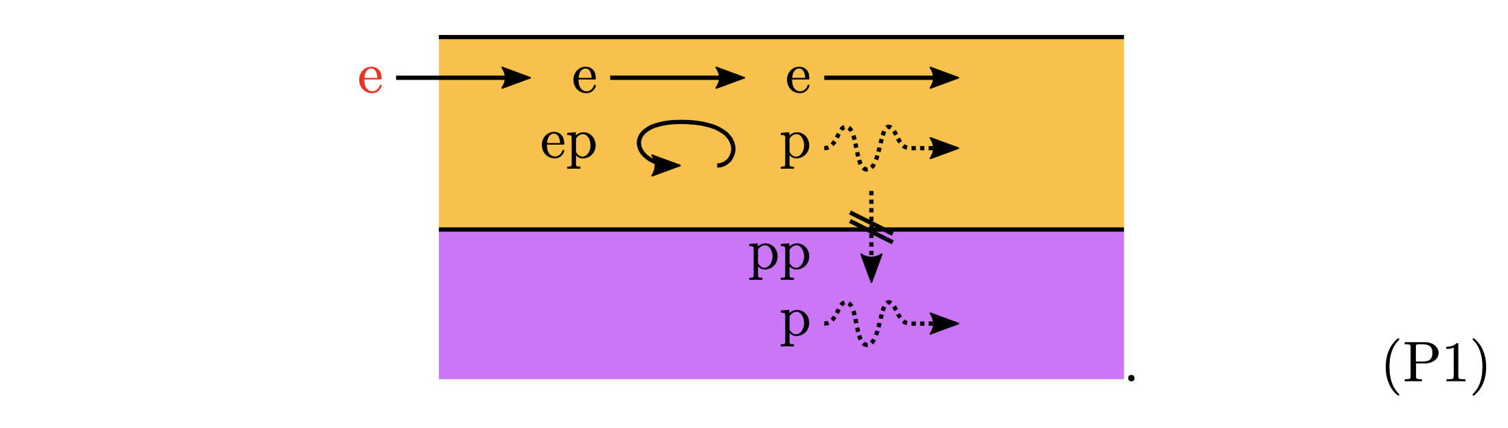
Heat goes through through the electronic bath, quantitatively described by the Wiedemann–Franz law [wiki], spreading out and warming up the metal. The electrons can not carry heat through and into the substrate, but inside the metal there is thermal coupling between electrons and phonons, the ‘e-p’ coupling. These phonons can also move through the metal, then after a bit of boundary resistance they can also enter the substrate. For now, we just assume that the phonons in the substrate are sufficiently connected to a cold bath. We can draw this as a diagram that connects different thermal bodies.

If we draw each connecting arrow above as a resistance in an rough electrical analogy we arrive at

where temperature is the voltage analogy and the source of heat is a driving current source towards a thermal ground. The heat will flow regardless of the thermal resistances, but will create a larger temperature gradient the larger the resistances are. But watch out, at low temperatures the thermal resistances are non-linear and multiple paths can complicate the model further.
With these ideas in mind, we can think about how geometry can maximize heat flow.
- The wider and thicker the trace is, the more heat can flow across it carrying heat away from the source with a smaller temperature gradient. The ee link in picture P3.
- The more voluminous the trace is, the more material for electron-phonon coupling to happen in. The ep link in picture P3.
- Then the larger the surface area of the trace to the substrate helps connect the trace to it’s heat sink. The pp link in picture P3.
- Finally, reducing the heat that the system needs to carry gives an obvious win. The current source in picture P3.
These four variables lead to some implementation ideas for cooler chips.
Isolation Routing
This method of wiring focuses on drawing the gaps between the traces rather than traces themselves. By carving out small gaps the total area of metal surface is maximized. Consider a hypothetical 6 point device (perhaps a hall bar measurement) with small wires connecting the bond pads to the device in the center,

but now maximize the metal coverage by routing the isolation instead,

that causes the ’wires’ to be large flat sheets. Inside the sheets of connecting metal there is lower electrical resistance, meaning greater thermal conductivity, as well as a larger volume which scales up the electron-phonon coupling. A caveat is the requirement to now consider crosstalk between the now closer lines. Isolation routing is inapplicable to transmission lines where the isolation is already a defined parameter.
Layer Thickening
Additional thickness of the metallic layers gives more volume for electron-phonon coupling in the same trace footprint,
There are lots of opportunities during fabrication, at sputtering / evaporation / plating where the thickness of the layer is not critical for the device. In these cases waiting longer in the process to fill up more of the available lithographic mask depth. Picking a thicker mask for even thicker traces or bond pads will further enable plating thicker layers.
A bonus is if you can plate materials with an intrinsic high electron-phonon coupling like gold.
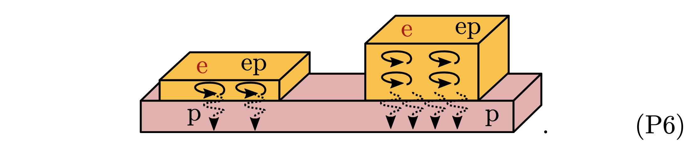
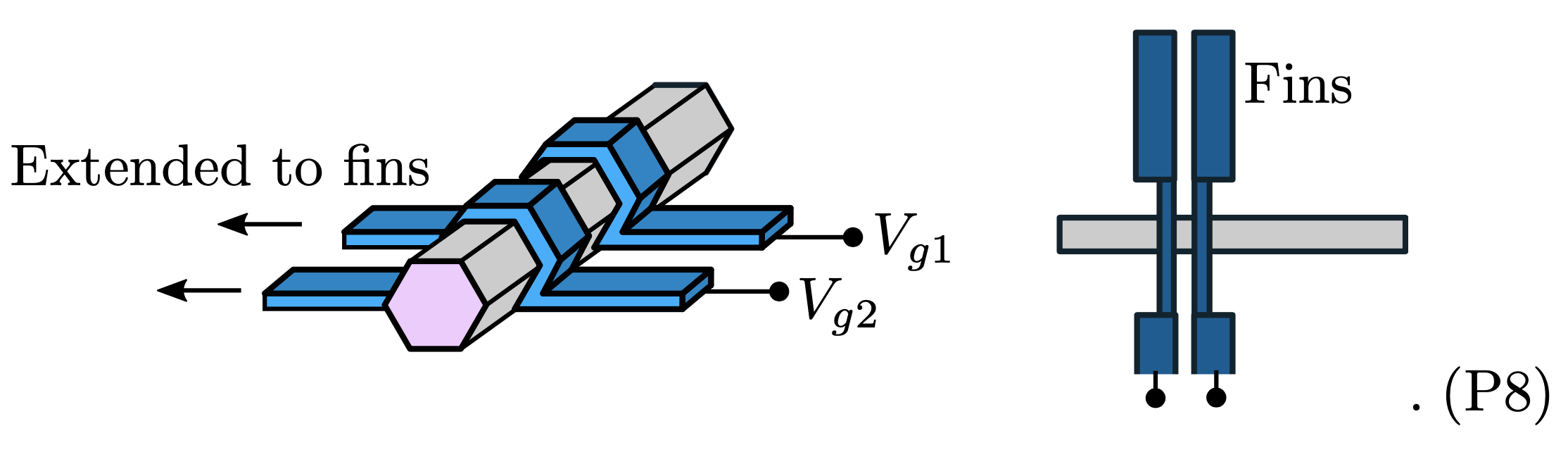
Cooling Fins
The cooling via the leads is likely blocked at the first high impedance section of the device. We can consider tens of milliohms as a high impedance for thermal resistances. Tunnel junctions, semiconductors, thin films, nanowires etc., all are good at stopping the flow of heat. These components can make sections of the device thermally isolated. Adding extra lines that don’t go anywhere, dead end traces, or cooling fins, just provide a thermal path for the isolated section to cool down, for example adding material between two tunnel junctions,
gives the electrons in the central section the ability to cool down. In these sections, where electrical transport of heat is bad, the coupling through the substrate becomes the dominating cooling path. The spur should do nothing for the electrical diagram, as it doesn’t connect to anything, but enhances the cooling for the isolated section. A trap would be accidentally enhancing the capacitive coupling around the device changing the charging energy of a dot or SET, or passing high frequency current around the junctions. There are more examples that can be pointless from an electrical viewpoint, but are good for thermals, like extending and fattening finger gates far beyond just the covering of a nanowire,
Enlarge Small Features Rapidly
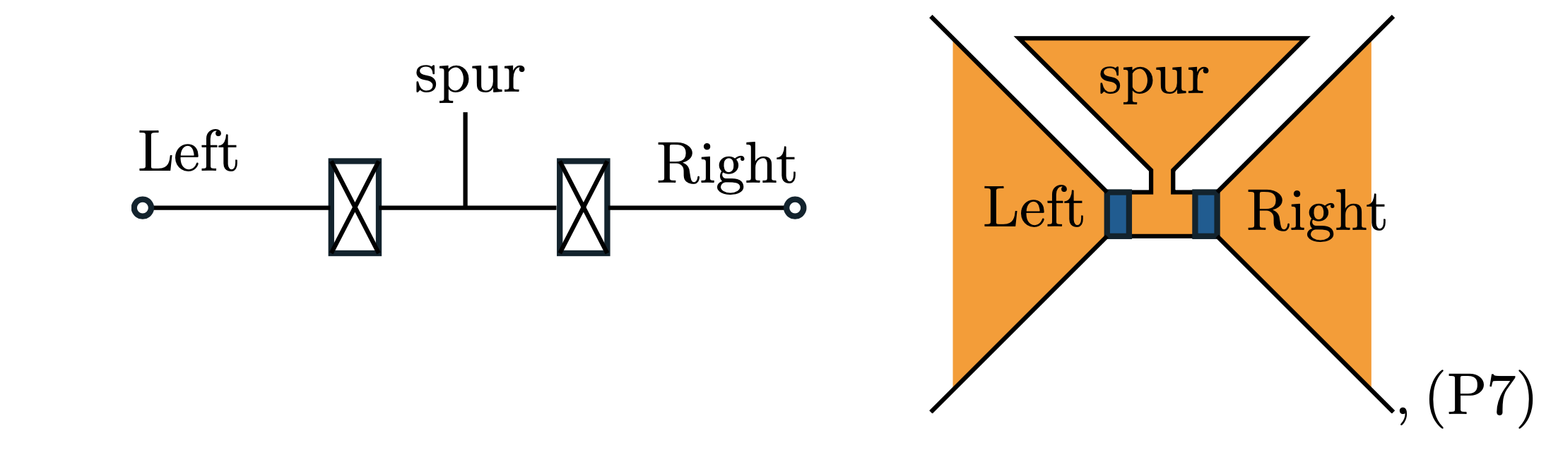
It is required that device connections are small, but not strictly that anything else is. We can expand the size of connections as soon as possible in a cone shape. Looking back at image P7 consider the expansion of the contact material.
A general technique to get nano-scale electronics cold is to get milli-scale as soon as possible.
If there are just two or four connection the device to line connections could look like
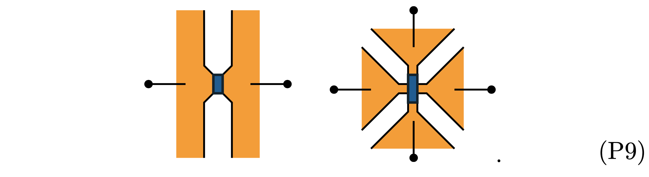
If you know some lines need to transport more heat, for example if they are current biasing, then one could prioritize the valuable surface area to these lines.
On-Chip Filters
Reducing the power that the chip needs to dissipate is an easy win for reducing the temperature gradients on chip. There are lots of tricks that can be applied to lines to filter out some unwanted frequencies, however as we do not want to dissipate additional power we limit designs to the dissipation-less category of filters, those focused on reflecting power or redirecting power. LC filters, Bragg filters [wiki], or just making big changes in the trace’s characteristic impedance can prevent power reaching the parts of the chip that do dissipate. By making the lines different shapes, the lines own inductance and capacitance can be exaggerated to form a simple LC filter like

The larger pad use capacitance to the ground plane under the chip and the thin sections enhance inductance. Using meandering inductors and finger capacitors can enhance the filtering further,

A final example; adding some capacitance between lines on chip can shunt noise away from the device.

This field of “planar filter structures” can get very interesting at higher frequencies, [wiki].
We have seen a few ideas that could be implemented in the design of devices that can help keep them cold. I have focused on ideas that should be easy to implement for low frequency devices. Notably it would be difficult to implement a few of these ideas for superconducting microwave electronics due to their stricter design limitations.
Summary
Knowing which thermalisation technique would open up the tightest bottleneck is a question answered by simulation and experiment, but if some techniques can be implemented for negligible cost and time then really why not. Hopefully the next time you open up your CAD program some thoughts of thermalisation cross your mind, and we can all get cooler chips in dilution refrigerators.
About the Author

Matthew Sarsby makes things truly cold for a living. After all, a quantum computer needs a quantum computer case too.